D.I.Y. 8M-Bit (1MByte) SEGA GAME GEAR Flash Cartridge
512KB Cart 8M-Bit Cart Cart PCBs -=GG PCB=-
Below you will find links to a Zip archives which include my schematic design & PCB layout.
Time permitting I will update this section with a Proceadures PDF. I will also put together an Instructional video for you to follow. Currently with my college schedule, I just don't have the time.So hopefully after this semester finishes I will post that for you all. So check back from time to time.
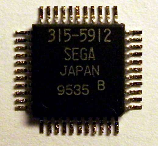
Below is a recent Schematic that I designed for this 1MByte Flash cart using the 315-5912 Mapper. I will soon be etching a Prototype PCB of this. However the PCB Layout is still in the design phase.
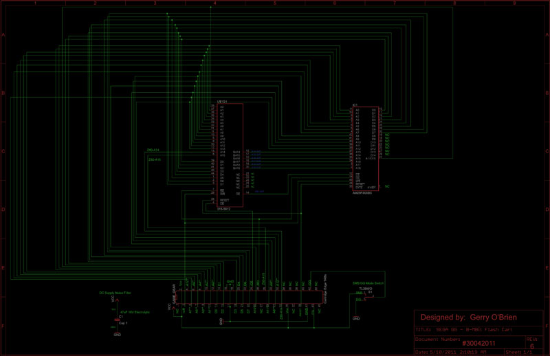
A few revisions are still required for this Schematic, such as GND lines and PADs. However it is 95 % completed.
NOTE: This design has already been tested and works without any issues. So you can use this Schematic as your wiring reference and as long as you match the connections as shown here, your cartridge will work without question.
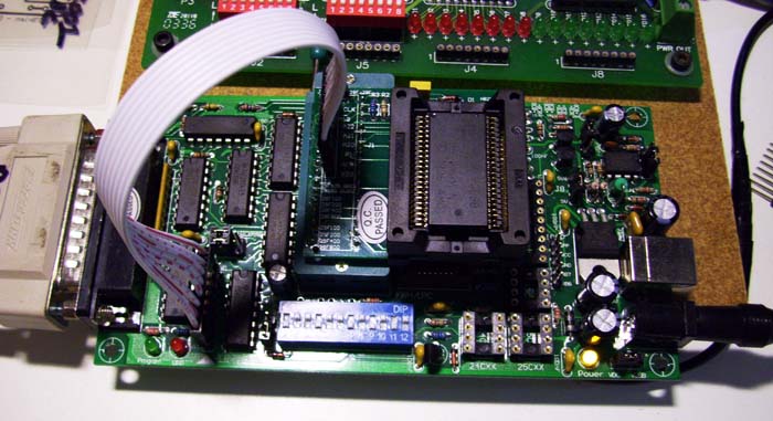
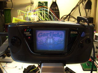
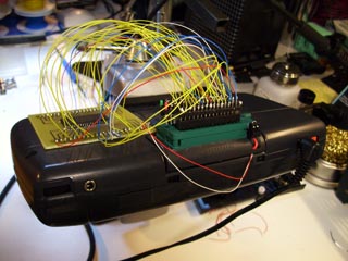
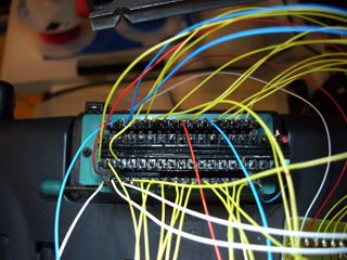
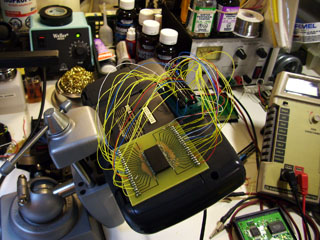
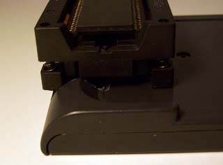
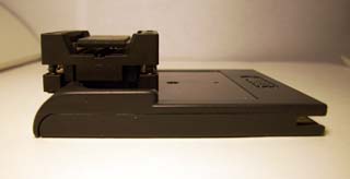
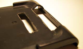
The Images below show the Interface Testing RIG I assembled while trying to map the proper Pinouts for the 8M-BIT Flash chip.
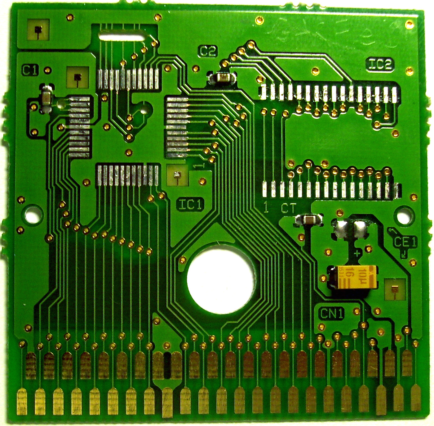
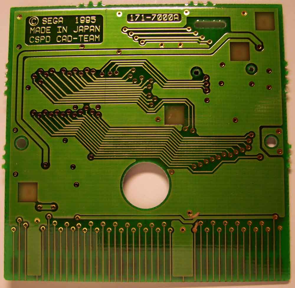
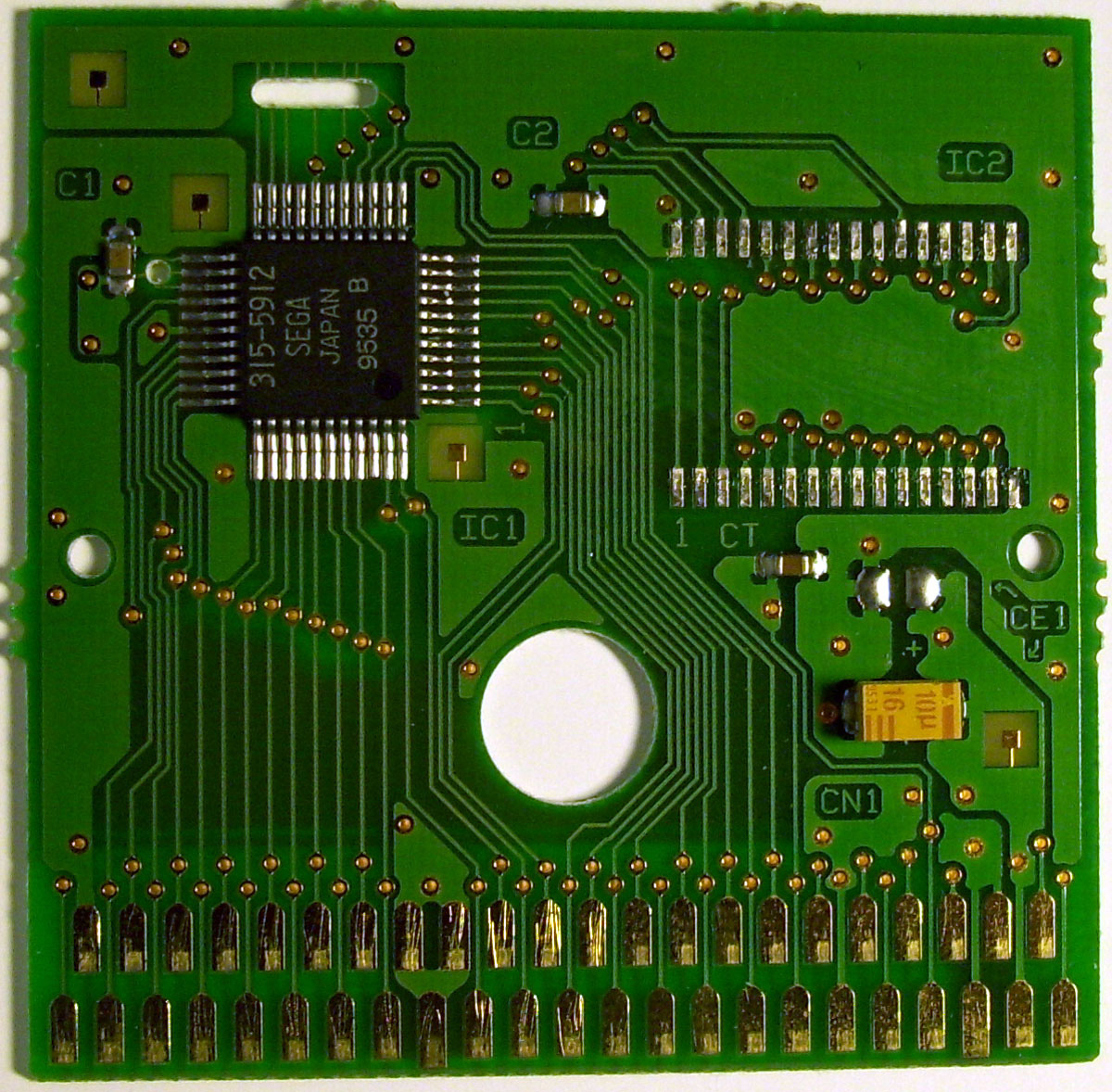
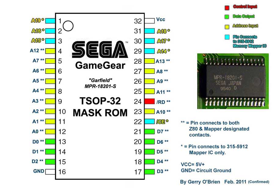
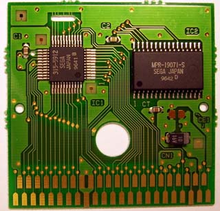
Now for this 1MByte version it is pretty straight forward. The first step is to simply de-solder the MASK ROM from an 8M-BIT Game Gear cartridge which has the 315-5912 Mapper chip. The cartirdge PCB is shown below. (SEGA Game Gear PCB Model # 171-7000A). The Schematic I posted above is essentially the Schematic diagram for the GG cartridge PCB shown below.
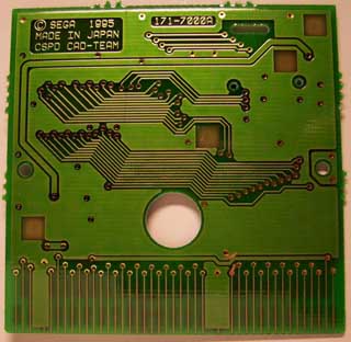
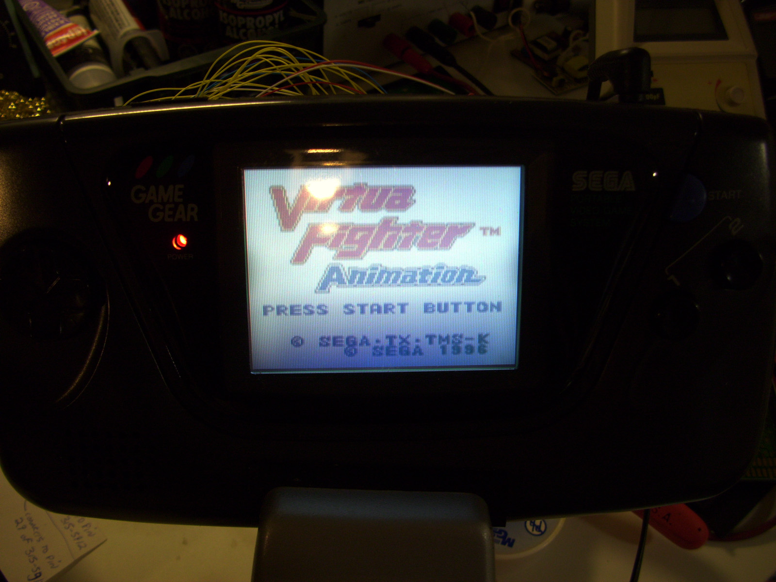
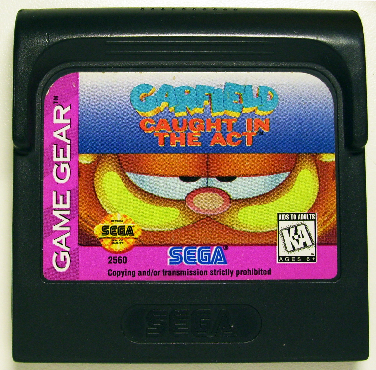
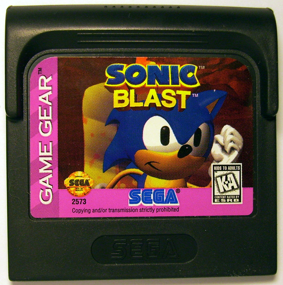
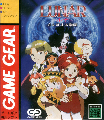
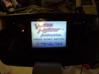
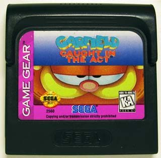
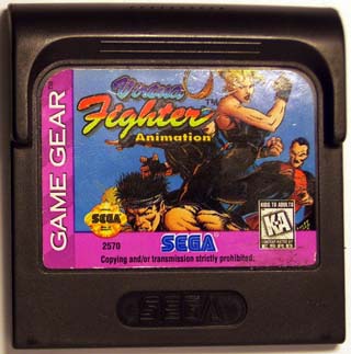
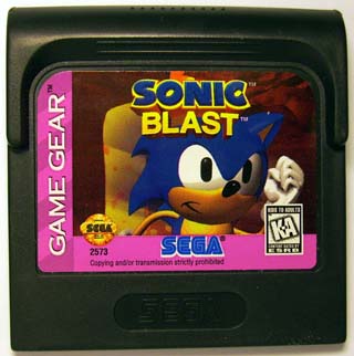
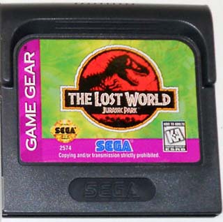
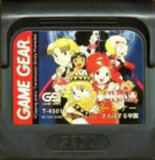
Other Game Gear Cartridges that use the 315-5912 Mapper chip and are of the same PCB design (Model #171-7000A), are shown below. You can also use these cartridges for this 1MByte Flash cart project.
- Garfield Caught in the Act & Virtua Fighter Animation.
- Sonic Blast & Jurassic Park - The Lost World
Import from JAPAN - Lunar Sanposuru Gakuen

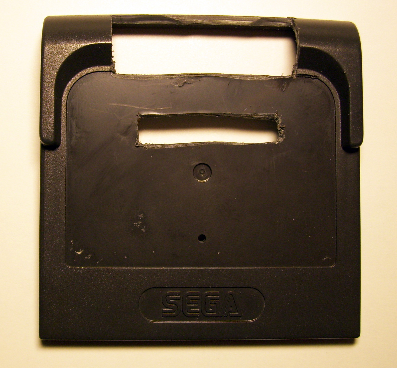
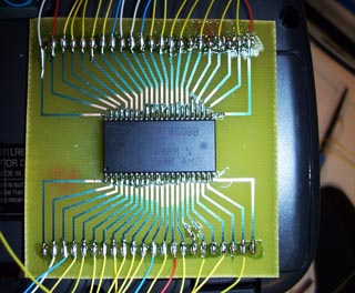
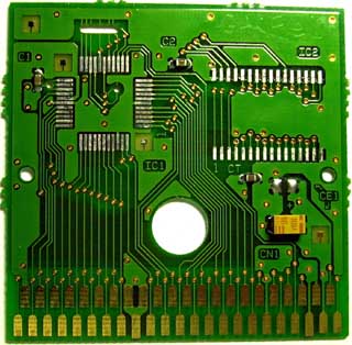
After desoldering the Mask Rom, you are then left with a GG PCB as shown below:

You must then Interface an 8M-BIT Flash chip (such as the AMD "AM29F800BB") in place of the MASK ROM. As long as you match the pin connections form the Flash chip to the MASK ROM Contacts on the GG PCB, according to the provided pinout diagrams (Links Below); you will not have any problems.
**Refer to the Schematic diagram to verify your connections.**
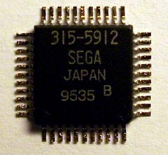
AM29F800BB Flash Chip for SEGA GG
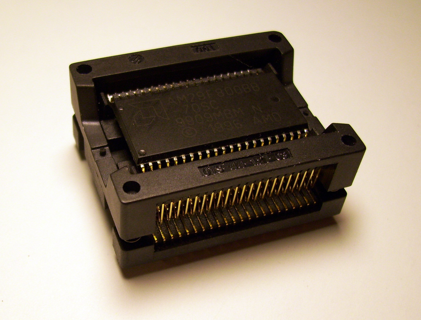
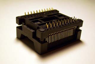
The main concern here will be your method used for programming the Flash chip. If you manage to purchase the required PSOP 44 Pin sockets for both your Willem Programmer and another to connect to your Cartridge PCB to accept the Programmed Flash chip, it will work just fine. Just remember that the pins on the PSOP type chips are very delicate and repetitive swapping may damage the pins if you are not careful.
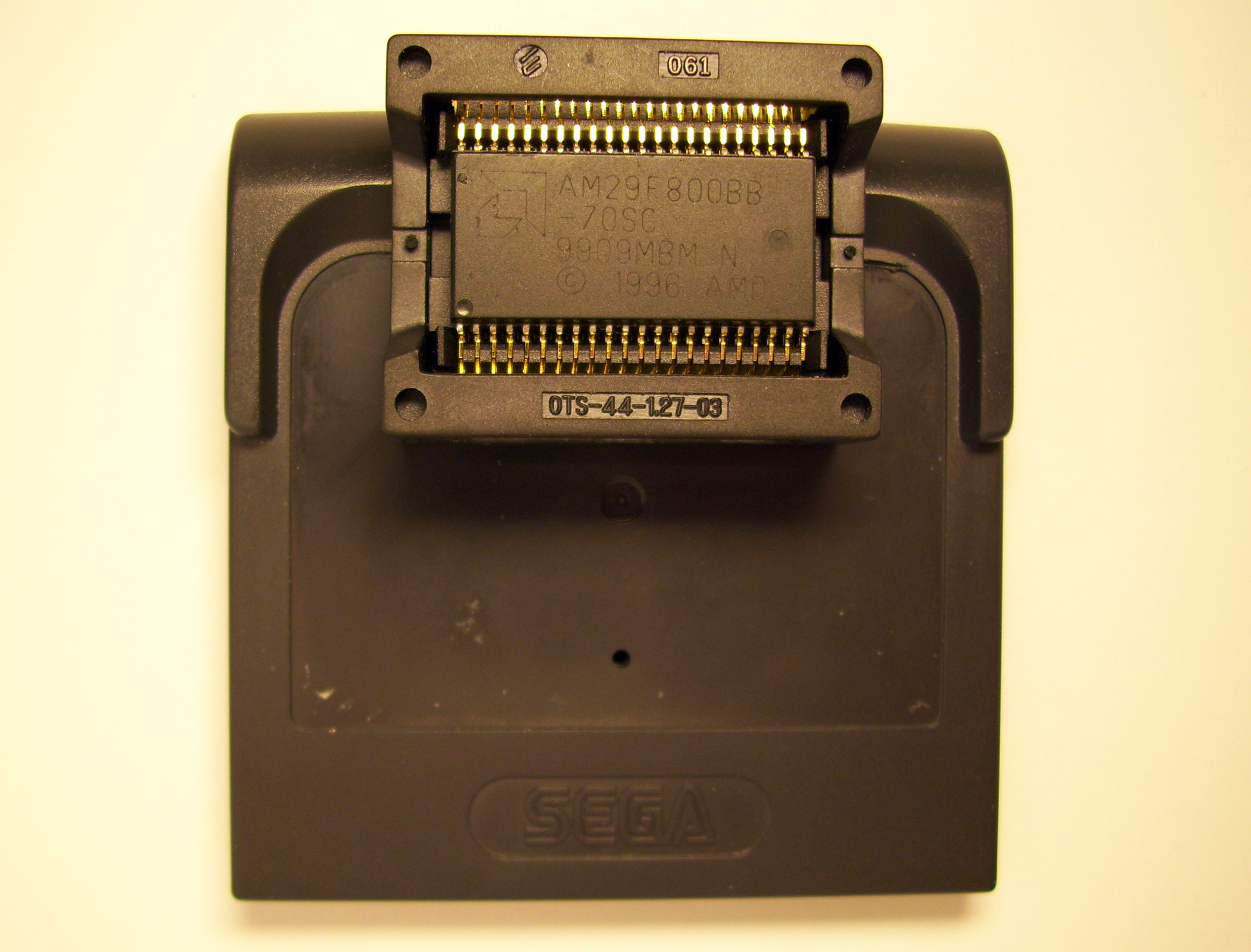
Below is an Image of the PSOP 44 Socket Adapter for the Willem Universal Programmer that accommodates the AM29F800BB flash chip.
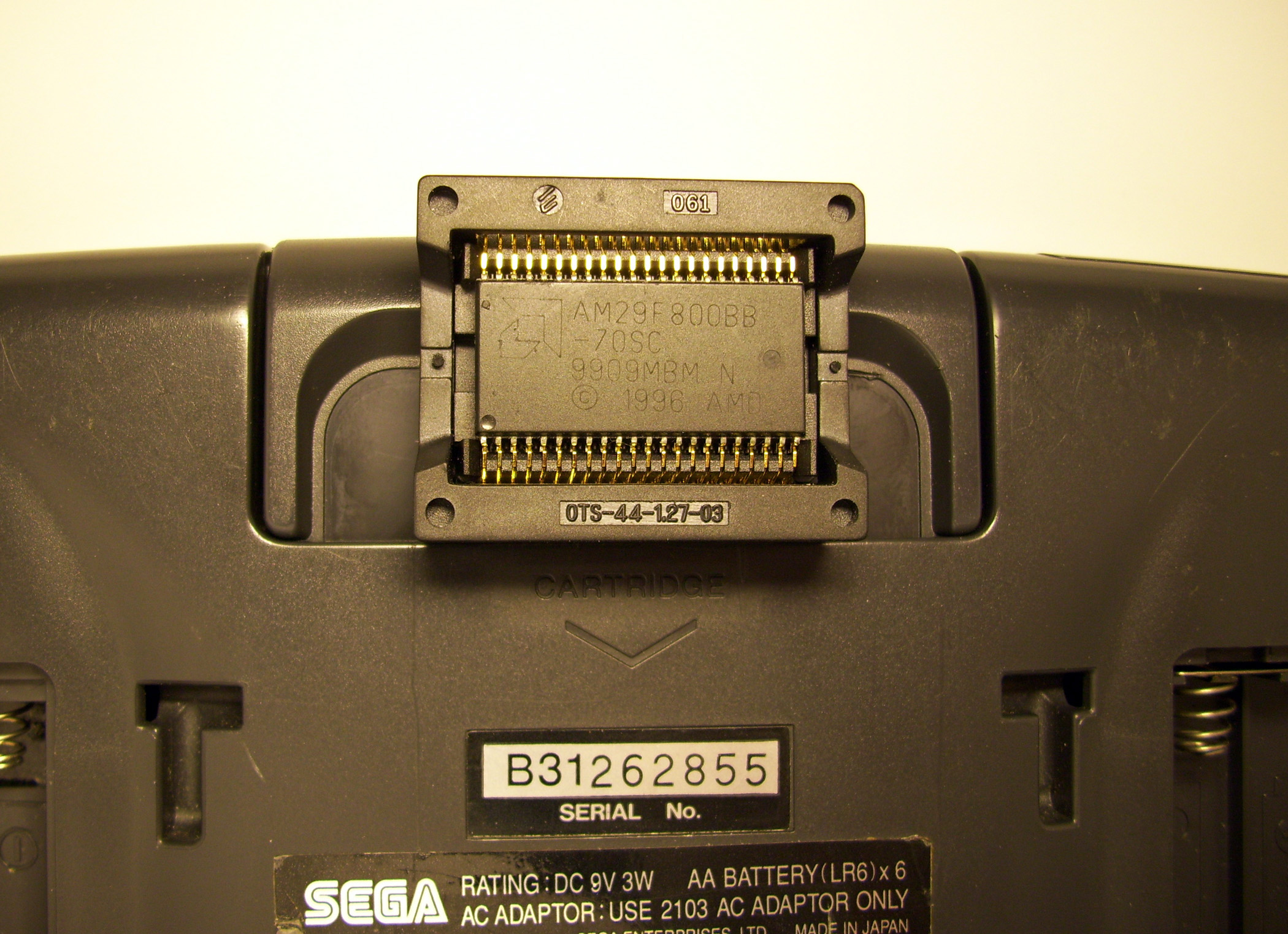
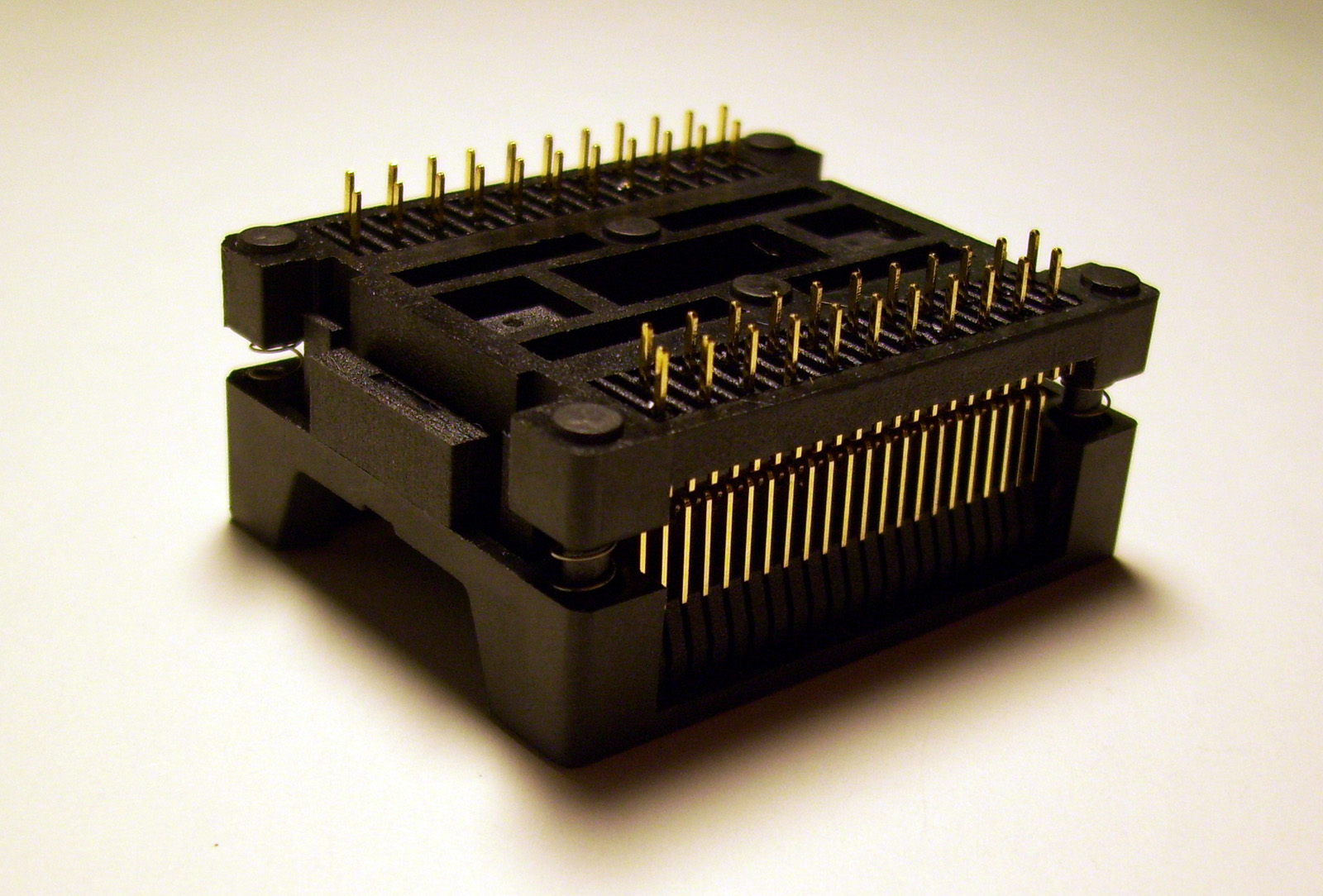
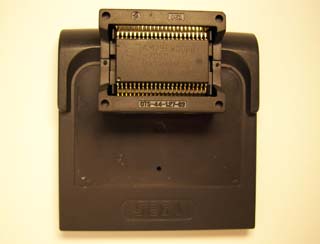
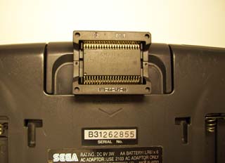
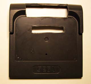
Shown below is my GG enclosure with the PSOP44 socket Adapter which makes it convenient for reprogramming.

The other alternative for programming your flash chip, is to build a custom programmer or a custom interface cable to connect to your Willem programmer. You can then have the PSOP Flash chip embedded inside the GG cartridge permanently and program it through the cable interface. But again as I mentioned earlier, this is another project on it's own and will not be discussed here.
Good Luck with all your Flash cart Projects Everyone!!
Kind Regards,
Gerry O'Brien