I have updated the VHDL code below just slightly, so it may appear slightly different compared to that which was shown in videos #1 and #2. However, 98% of it remains the same. Reason for these changes... I revised the code to help explain the timing and clock signals required to drive the LCD CORE State Machine. In the 3rd Video, I focus on explaining why a "400Hz ENABLE" signal was used to drive the LCD core State Machine. The changes I have made are minor and are explained in the 3rd video posted above.
I have added detailed comments in the NEW VHDL code below... to at least explain what is going on. However if you are still confused, rest assured...in the 3rd video, I go over everything regarding the Timing and the Clock signals in great detail. This will help solidify your understanding.
So definitely check it out. :)
VHDL CODE UPDATED: JULY/24/2016
PORT DECLARATIONS
(Pin Planner Pin assignments)
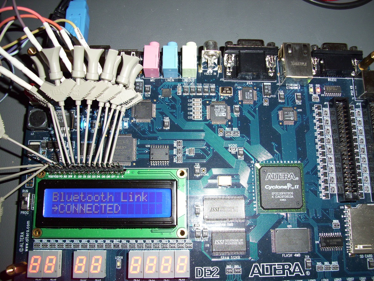
The following Port Declarations are setup for the Altera DE2 Cyclone II FPGA Model# "EP2C35F672C".
TIMING AND WAVEFORMS & LOGIC ANALYZER SCANS
FOR VIDEO #1 and #2
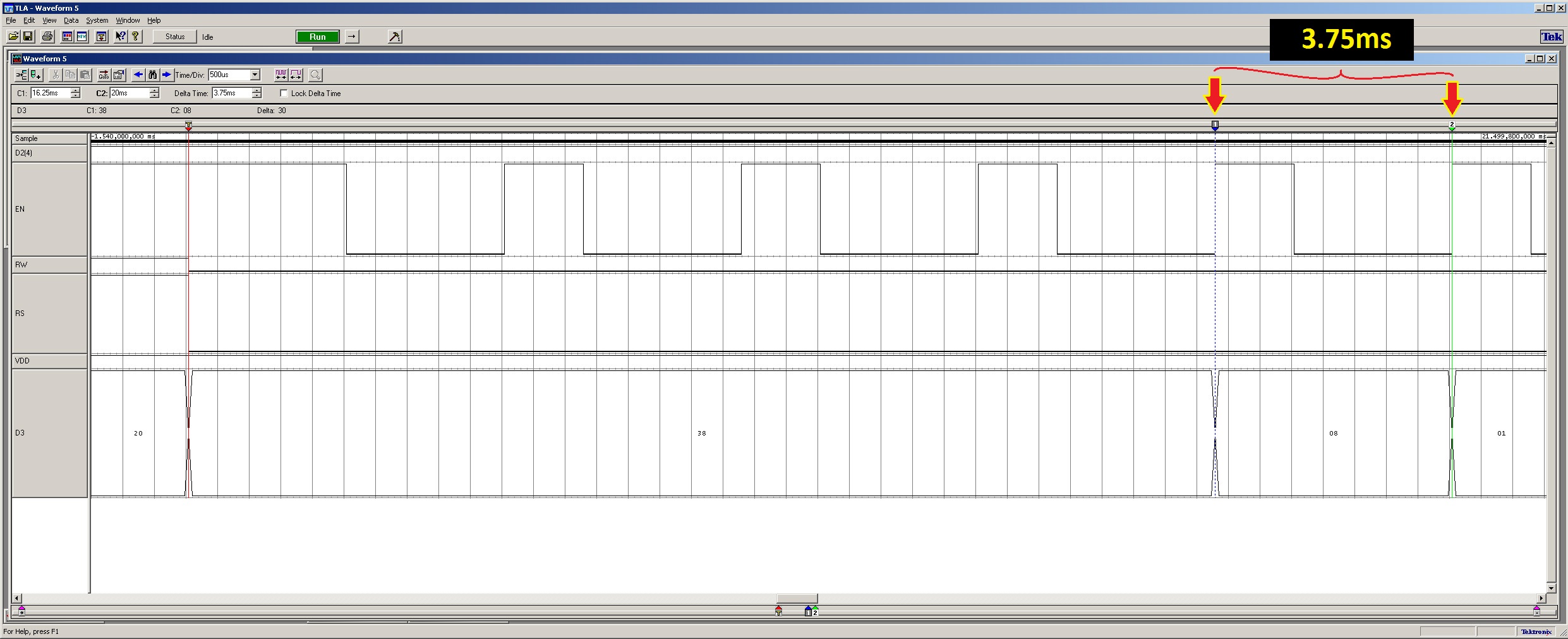
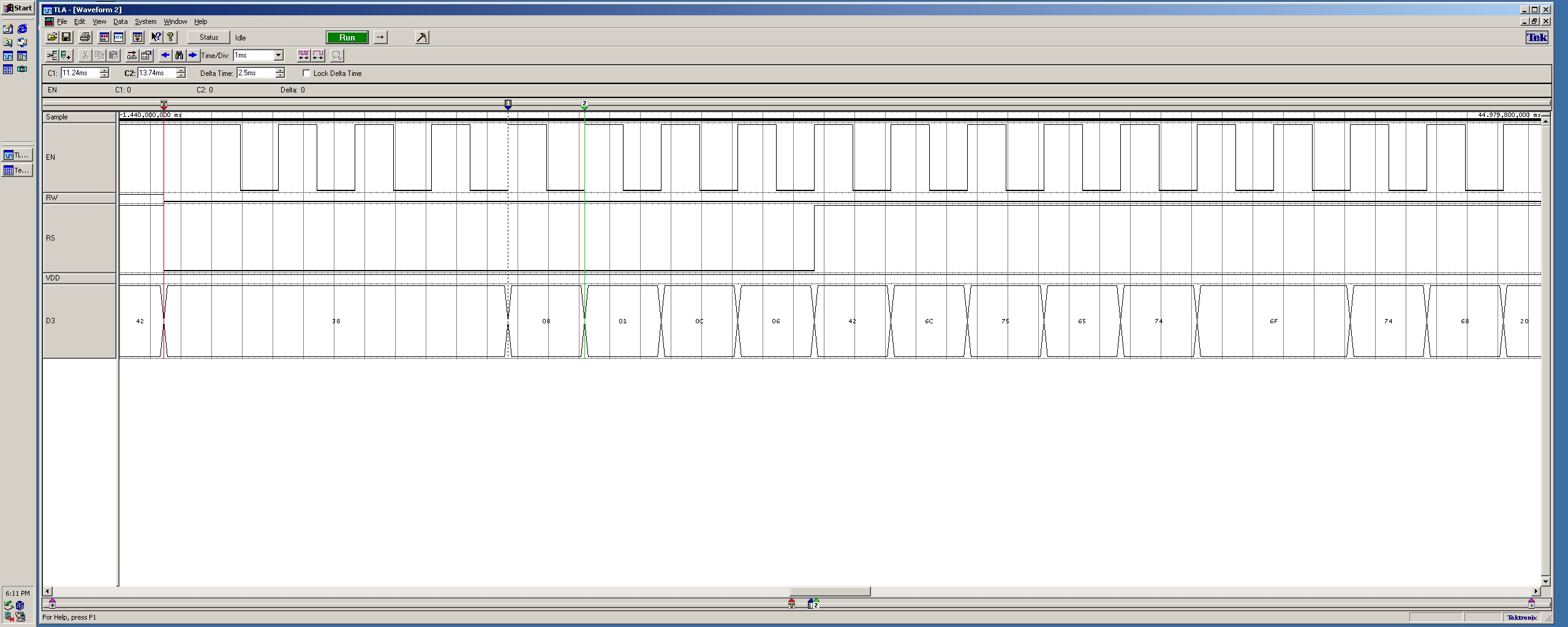
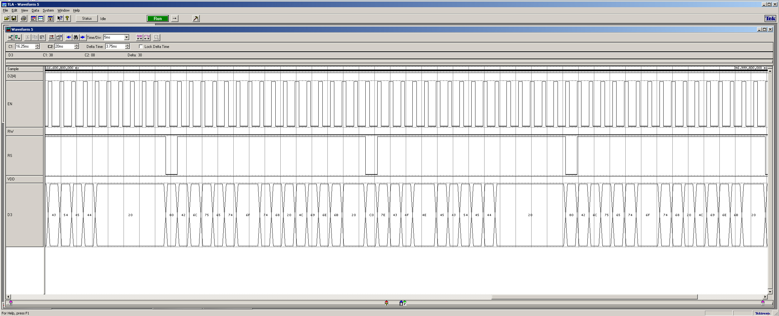
Shown below are screenshots of the Logic Analyzer scans used in the instructional videos #1 & 2.
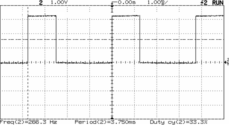
Using the original VHDL code as shown in Videos #1 and #2, the LCD's "ENABLE" line and DATABUS signals are made up of 3 STATES from the LCD core State machine. Using the DE2 DEV. boards 50Mhz Clock to trigger (x3) cycles of this State machine; creates the period of 3.75ms for both the DATABUS and the LCD "ENABLE" line. This also creates a duty cycle of 33.3% and a frequency of 266 Hz for the LCD "ENABLE" LINE specifically.
clk_count_400hz <= x"0F424"
50Mhz/800hz = 62500 converted to HEX = F424
800hz/3 STATES = 266 Hz
100% Full Cycle/3 STATES = 33.3333% DUTY CYCLE
(We have a 33.3% Duty Cycle as the signal is only Logic Hi for 1 of the 3 states. Or is Logic Hi for 33.3% of the Full Cycle.)
(Notice the Period of 3.75ms)
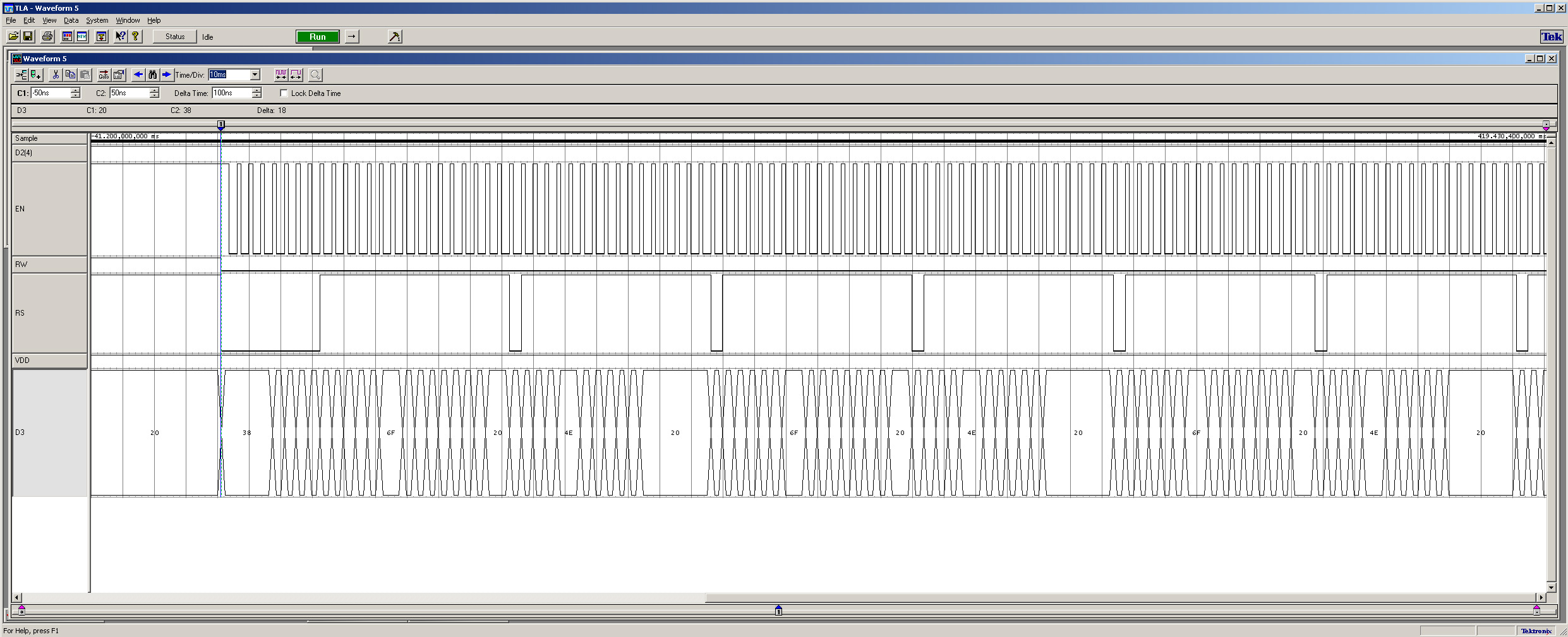
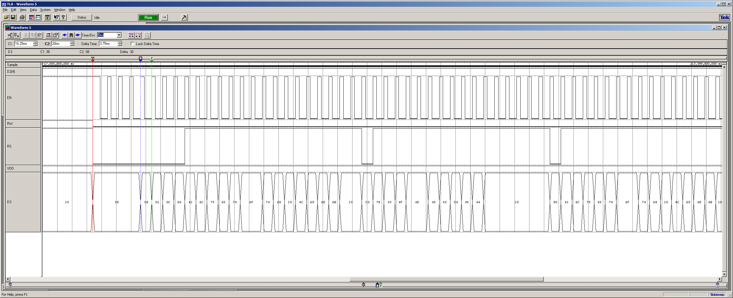
TIMING AND WAVEFORMS & LOGIC ANALYZER SCANS
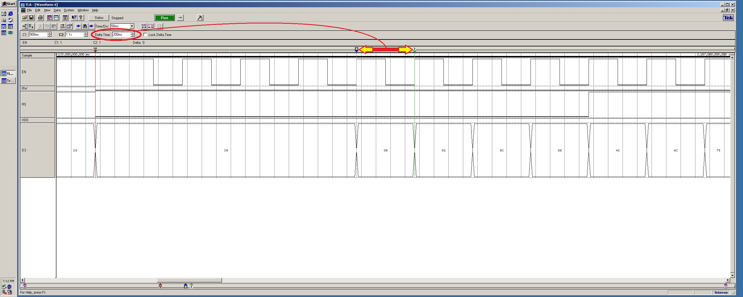
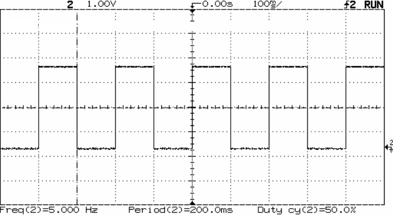
FOR VIDEO #3
clk_count_400hz <= x"4C4B40"
50Mhz/10hz = 5000000 converted to HEX = 4C4B40
10hz/2 STATES = 5 Hz
100% Full Cycle/2 STATES = 50% DUTY CYCLE
(We have a 50% Duty Cycle as the signal is Logic Hi for 1 of 2 states. Or is Logic Hi for 50% of the Full Cycle.)
(USING THE NEW VHDL CODE!!! - Notice the Period of 200.0ms)
clk_count_400hz <=x"00F424"
50Mhz/800hz = 62500 converted to HEX = F424
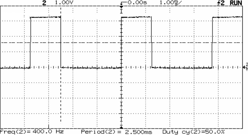
800hz/2 STATES = 400 Hz
100% Full Cycle/2 STATES = 50% DUTY CYCLE
(We have a 50% Duty Cycle as the signal is Logic Hi for 1 of 2 states. Or is Logic Hi for 50% of the Full Cycle.)
(USING THE NEW VHDL CODE!!! - Notice the Period of 2.5ms)
This is the intended signal that the Original LCD CORE was designed for, and this is why the Counter Variable "clk_count_400Hz" was being used. They intended that the end result would be a frequency of 400Hz for the LCD's "ENABLE" line.
LOGIC ANALYZER SCANS FOR VIDEO #1 and #2
(Full Zoom out showing the logic signals repeating.)
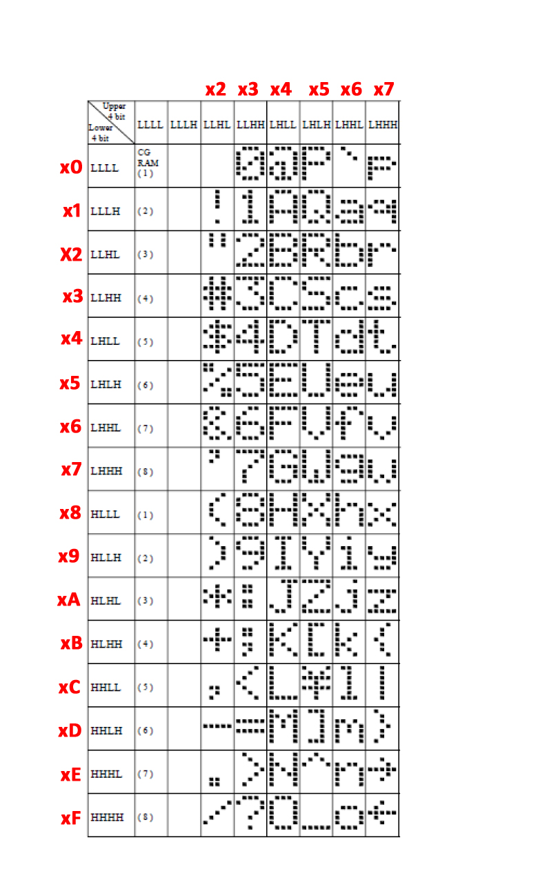
Start of LCD Initilization and display process. (Zoomed in)