Here we will discuss The "JTAG" IEEE 1532 standard used for "ISP" (In-System-Programming)
I will also talk about Atmel's "AVR ISP" programmer and it's "SPI" (Serial-Peripheral-Interface).
Using the Altera USB Blaster
For programming Altera FPGA & CPLD components
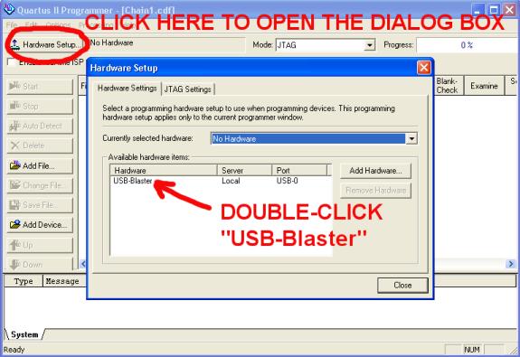
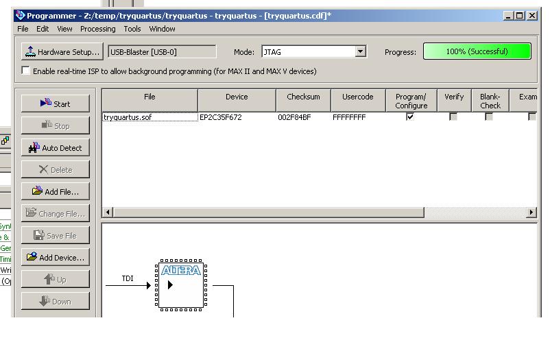
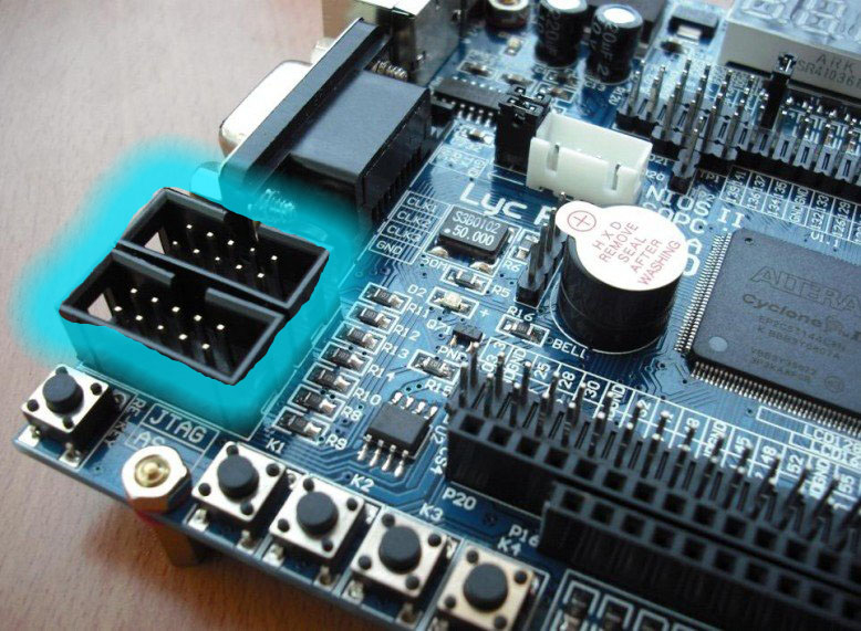
You are probably familiar with the process of programming your Altera development board (Altera DE1 or Altera DE2) by using the Altera "USB-Blaster" hardware setting, within Altera's Quartus II Programmer software as seen in the image captures below.
You may never have really thought about how the signals from the USB cable actually interface to the FPGA chip.
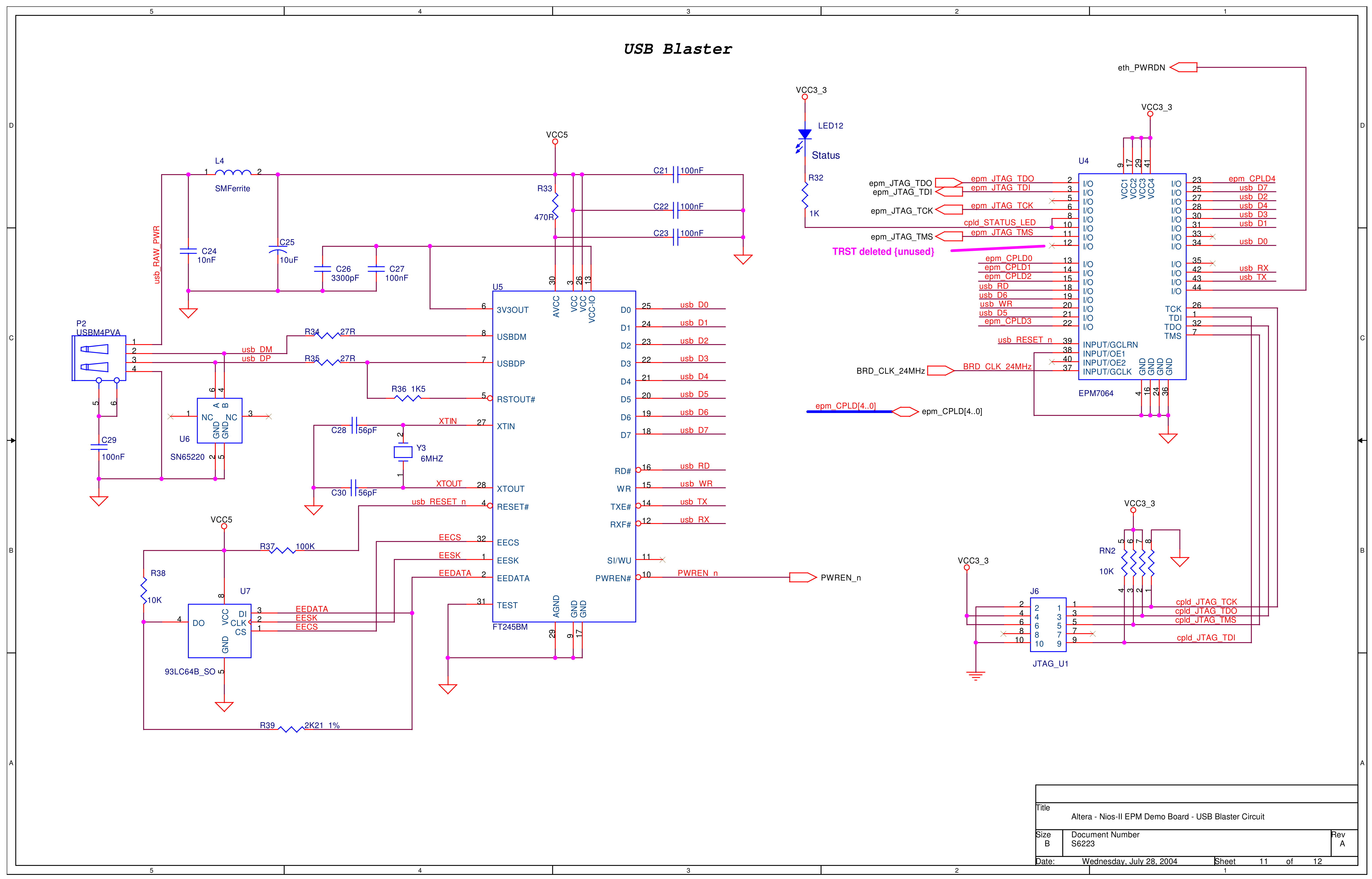
Well, the fact is that your Development board is equipped with a built-in Altera "USB-BLASTER" programmer circuit also known as a JTAG controller. A schematic diagram of such a controller is shown below:
From the edaboard.com forum , Ozzie poster "cube007" provides a schematic diagram of the Altera USB-Blaster JTAG programmer.
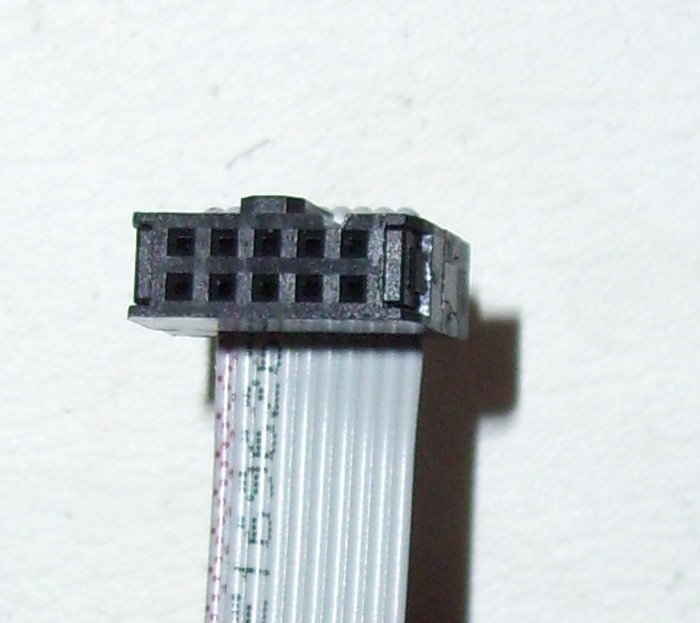
This Programming interface circuit sends the programming signals from the USB cable to the FPGA chip directly, through a standardized 10-PIN interface. Technically there are only 4 or 5 signal pins used, excluding GND and unused interface pins from the 10-PIN Ribbon cable that is commonly used by JTAG controllers. Almost all FPGA and CPLD components have a set of devoted pins on the chip for this JTAG "In-System-Programming" interface.
Technically this 4 or 5 pin interface depending, is called a "TAP" or Test-Access-Port but, it is most commonly referred to as simply the "JTAG INTERFACE".
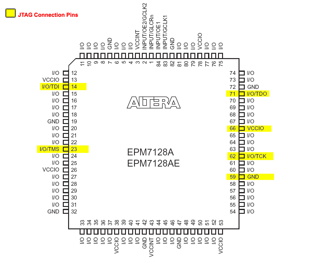
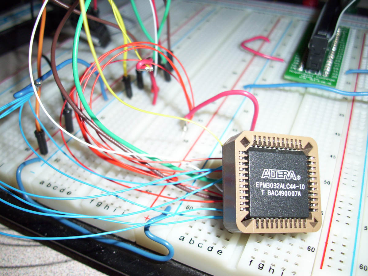
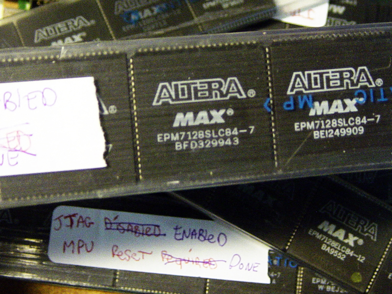
Here below is an older Altera MAX7000S CPLD chip which supports this JTAG interface used for special applications including a feature called "ISP" or In-System-Programming. I have highlighted the JTAG interface pins in Yellow for your convenience. So all that is needed in order to program this chip, is to connect these JTAG pins from the chip to a USB-Blaster circuit. You then also connect all of the chips VCC and GND pins to source power and.......
......Voila!
The chip is now ready to be programmed In System via the Altera software.
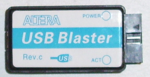
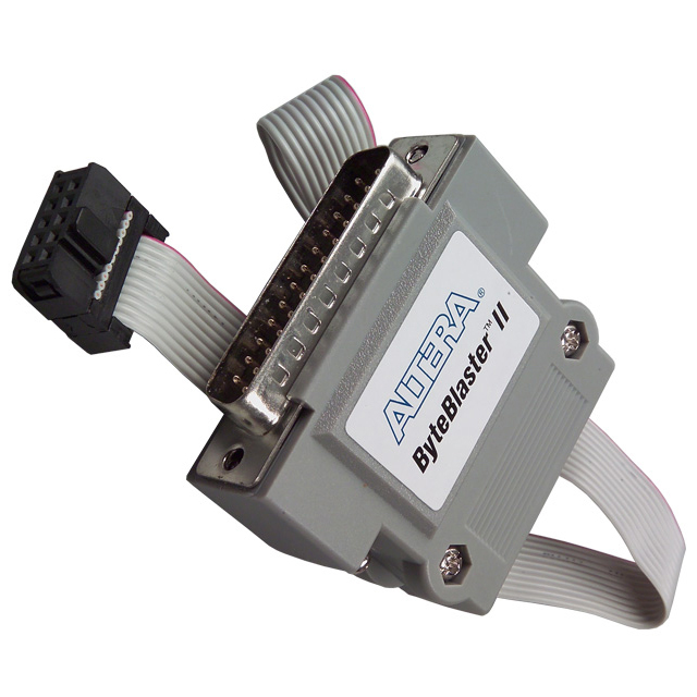
Altera USB Blaster external programmer
The USB-Blaster or "JTAG" programming circuit is also available as an external JTAG controller called the "ALTERA USB-Blaster" as seen in the images below. There was an older version of this JTAG controller called the Altera "BYTE-BLASTER-II" and it connected to your PC's 25pin Parallel printer port.
Having this "USB-BLASTER" JTAG controller gives you the option to program other CPLD's and FPGA's that provide the JTAG interface and support the "ISP" (In-Service-Programming) feature.
In turn, you can build your own PCB's and program an Altera CPLD or FPGA device with your own logic design. The chip is programmed the same way you program your Altera development board through Quartus or your logic Synthesis software of choice.
Pretty AWESOME!!
Many of the older Altera CPLD chips require a special Master Programming unit, in order to be programmed and do not support the JTAG interface at all. The reverse is also true, for instance the Altera MAX II family of chips can only be programmed via a JTAG interface.
Most educational Development boards will have the JTAG port available for programming your target device, or it may be built right into the development board itself and all you need to do is connect a USB cable to commence programming. Now if you are etching your own PCB's, you can build your own ISP programming interface using a JTAG programming device; such as the Altera "USB-BLASTER" or the "ByteBlaster II".
These Altera USB JTAG controllers vary in price, but are commonly available between $10.00 & 30.00 US dollars depending on the distributer. They are available from Amazon.com from the link below:
They are also widely available on eBay from various sellers all over the world.
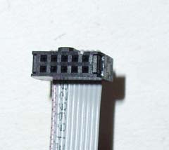
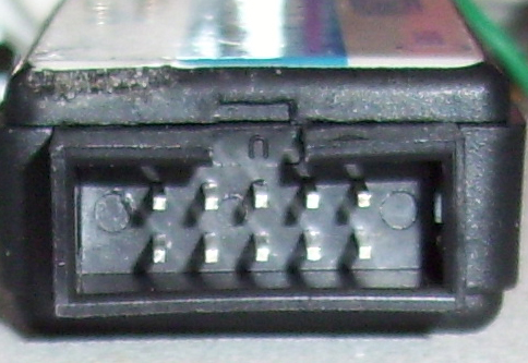
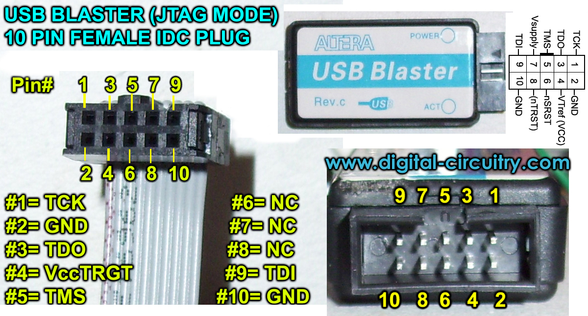
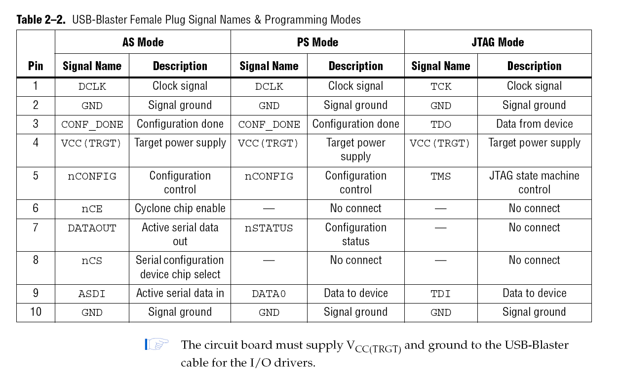
The Pinouts for the ALTERA USB-Blaster controller in the "JTAG IEEE 1532 Standard" Mode is shown in the image below.
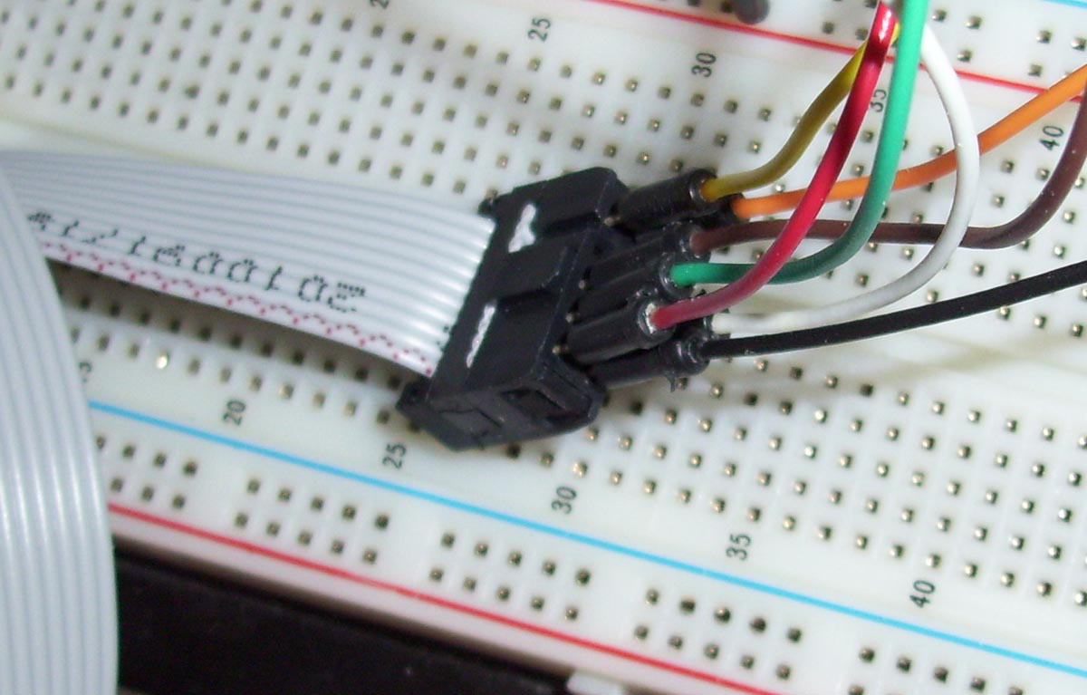
This will allow you to build your own custom circuits & program various logic devices as shown in the photos below. You could also integrate a 10-pin programming port on your own PCB design to connect the USB-Blaster's IDC ribbon cable to integrate JTAG ISP programming to your projects.
The Altera USB-Blaster is also able to program special Altera serial devices In-System, using two other programming modes known as the "AS" Mode (Active Serial) and "PS" Mode (Passive serial). You can use the chart below for the proper Pin connections for these Altera serial programming Modes.
The JTAG Controller has many IEEE standards that it supports.
The JTAG IEEE Standards:
After further development the "Join Test Action Group" found that the JTAG controller could be used for a number of different applications such as device programming. They decided to assign development teams to each of the various applications that the JTAG controller could be used for. Once perfected they Standardized each group as an IEEE standard.
IEEE 1149.1 = "JTAG Boundary Scan" for digital circuit testing.
IEEE 1149.6 = Adds support for AC coupled nodes like LVDS (Differential Signaling to remove noise from the comm lines)
IEEE 1149.7 = Decreases the pin count on the TAP interface from five pins down to two.
This scheme reduces the number of pins needed on the IC for control and test.
IEEE 1532 = (ISP) An enhancement to 1149.1 was developed around the year 2000 to standardize the methodology for programming these types of devices. With IEEE 1532, compliant devices, regardless of vendor, may be configured (written), read back, erased and verified, singly or concurrently.
If you wand to learn more about the JTAG Boundary Scan IEEE 1149.1 Standard, you can visit the webpage here on my website at the link below.
The JTAG IEEE Standard 1532 is also referred to as "ISP"
Remember "ISP" stands for "In-System-Programming" and is a "Feature" of a device that allows a device to be programmed while it is "In-System" regardless of the manufacturer.
The JTAG group declared the particular JTAG Standard "IEEE 1532" as "ISP". This is the JTAG standard that is used to program CPLD's and FPGA's "In-System".
How creative of them! LOL! :)
The JTAG IEEE 1532 standard that is used by Altera components, is a communication mode that uses the JTAG interface of 5 Pins (10 Pins on the standard Ribbon cable IDC connector) this allows users to program the target chip very quickly and with ease. Now, the JTAG controller can also be used for hardware testing, which is called the "JTAG Boundary scan" and is another IEEE standard. This Standard is entitled "JTAG IEEE Standard 1149.1" which is the initial reason the JTAG controller was developed. These are probably the two most popular JTAG Standards used today.
"JTAG" stands for "Join Test Action Group". This is the development group who designed the JTAG controller circuit for Testing and Programming CPLD's and FPGA devices. It was originally designed to be used as a Hardware testing circuit and interface, for the rapidly advancing Logic Devices that were getting smaller and smaller every day. In turn, fewer PCB test points were available as most of the digital circuitry was residing within the CPLD components. Also, multi-layer PCB's are constantly becoming more and more densely populated with interconnections and layers.
Connecting probes for testing the hardware was no longer possible because of their small size, and an ever growing problem for mass production testing. BGA components where contacts are hidden under the Chip and inaccessible, presented yet another problem for testing. A form of testing these circuits and Logic devices for faults had to be developed.
This was the reason the "Join Test Action Group" was formed and they released the "JTAG IEEE 1149.1" Standard
A.K.A. "JTAG Boundary Scan" to perform this hardware testing.
For further details on the JTAG Boundary-Scan "JTAG IEEE 1149.1" Standard, visit the links below:
JTAG programmers and Atmels "AVR ISP" programmers do not use the same interface.
DO NOT Get the JTAG Controller unit mixed up with Atmel's "AVR ISP" device programmer.
This is a completely different system for programming Atmel micro-controllers!!
Now, there is another completely different type of device programming controller called "AVR ISP" used by Atmel components and micro-controllers. Many users confuse this controller with the JTAG controller. It uses a different type of communication Bus entirely and so the interface Pinout assignments are different and incompatible. So don't get these two programmers confused.
What's the difference between these two interface ports?
Of course this is where a lot of confusion set in and why many users assumed that JTAG controllers & Atmels "AVR ISP" programmer unit used the same interface.
These are Two separate types of interface's used in Hardware programming.
Some Atmel "AVR ISP" programmers come embedded with the ability to program JTAG ISP supported components for convenience.
Now one thing I want to clarify is the terminology of "ISP" & "SPI" and what they are.
You have to realize that ISP is a feature of a device that allows the component to be programmed in System.
ISP = In-System-Programmable
This is a "FEATURE" that applies to many components of different manufactures.
For Example, Altera components can be programmed In System using the JTAG interface that is shown in the image above. Other components could use other interface ports to program the chip "In System" in the same way as the JTAG interface for Altera components.
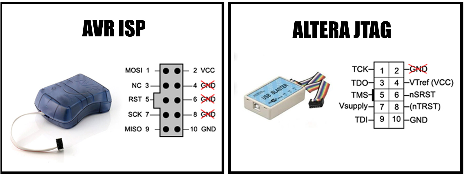
Now, the Atmel "AVR ISP" programmer unit shown in the picture above uses an INTERFACE called "SPI" or Serial-Peripheral-Interface
SPI = Serial-Peripheral-Interfacee
This is the interface shown in the Image above with the ATMEL AVR ISP Programmer unit.
The SPI Interface comprises the following pins:
- MOSI
- MISO
- RST
- SCK
The Altera USB-BLASTER programmer unit shown above uses an INTERFACE called the "JTAG INTERFACE" or "TAP" for Test-Access-Port.
This is the interface shown in the Image above with the ALTERA JTAG USB-BLASTER Programmer unit.
The Altera "JTAG INTERFACE" or TAP (Test-Access-Port) comprises the following pins:
- TCK
- TDO
- TMS
- TDI
So just to be clear:
ISP (In-System-Programmable) = A "FEATURE" of device regardless of the manufacturer. Altera, Xilinx, Atmel ect. all support the ISP feature for various components they sell.
SPI (Serial-Peripheral-Interface)= A Hardware Interface commonly used by Atmel Micro controllers.
JTAG INTERFACE= The Hardware Interface used by JTAG programmers. Commonly used to program CPLD's and FPGA's and perform hardware testing using Boundary scan software. This interface is technically called the "TAP" or Test-Access-Port. However, it is most commonly referred to as simply the "JTAG INTERFACE" especially by first year students.
For Information on ATMEL's AVR ISP interface & MKII Programmer visit the link below:
FEWWWWW!!!! Glad I got that confusion out of the way.
What I am about to discuss below is an important fact to remember, and many Hobbyists don't realize or bother to think about. So Pay attention and remember the following....
"Altera MAX 7000 PLCC chips are the "PERFECT SIZE" for working on with our Human hands."
The older Altera MAX 7000 family of CPLDs should be the CPLD's of choice for electronics hobbyist; due to the fact they are released in the "PLCC" package format, which is the "PERFECT SIZE" for working on with our Human hands. They are also extremely Robust compared to delicate Surface mount components.
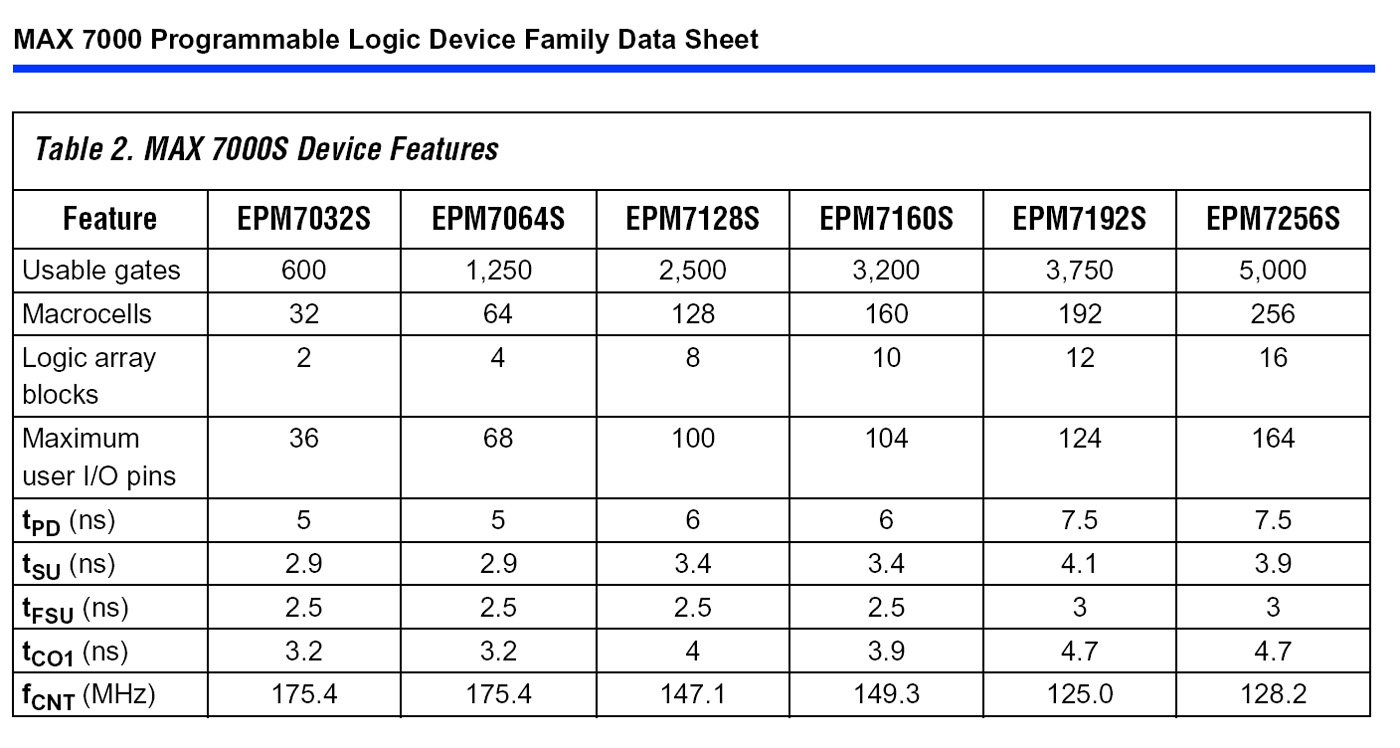
You can get an 84-pin PLCC Altera chip (Altera Part# EPM7160SLC84-10) which has 160 "Macro-cells". Macro-cells are essentially a type of Customizable Flip-Flop. This chip has an equivalent count of 3200 Logic Gates. This will allow you to program a larger design into the CPLD compared to smaller Macro-Cell count chip. Like the ALtera EPM7128SLC84-10. This chip has 128 Macro-cells and an equivalent count of 2500 Logic Gates. I have provided the Altera MAX 7000S Gate count chart which shows the Maro-Cell and Gate count according to the Altera Part number. This chart is available within your Components Data Sheet.
Altera FLEX and STRATIX Family chips have up towards 10,000 or 20,000 Logic Gates, and are a better choice for larger designs. However most of these Chips are either only available in PQFP or TQFP surface mount packages, with at least 160 pins. For smaller Hobby based projects, the 84-pin PLCC package Altera MAX7000S chips are a better choice, as they are easier to work with on the Bench.
Now, the Altera DE1 boards "Cyclone II" FPGA chip has 20,000 LE's (Logic Elements). LE's contain a 4-input "LUT"(Look up Table) that can create customizable Flip-Flops similar to how Macro-cells do, but they are inter-connected inside the chip in a different way. Regardless, they perform a similar function just like the Macro-cell.
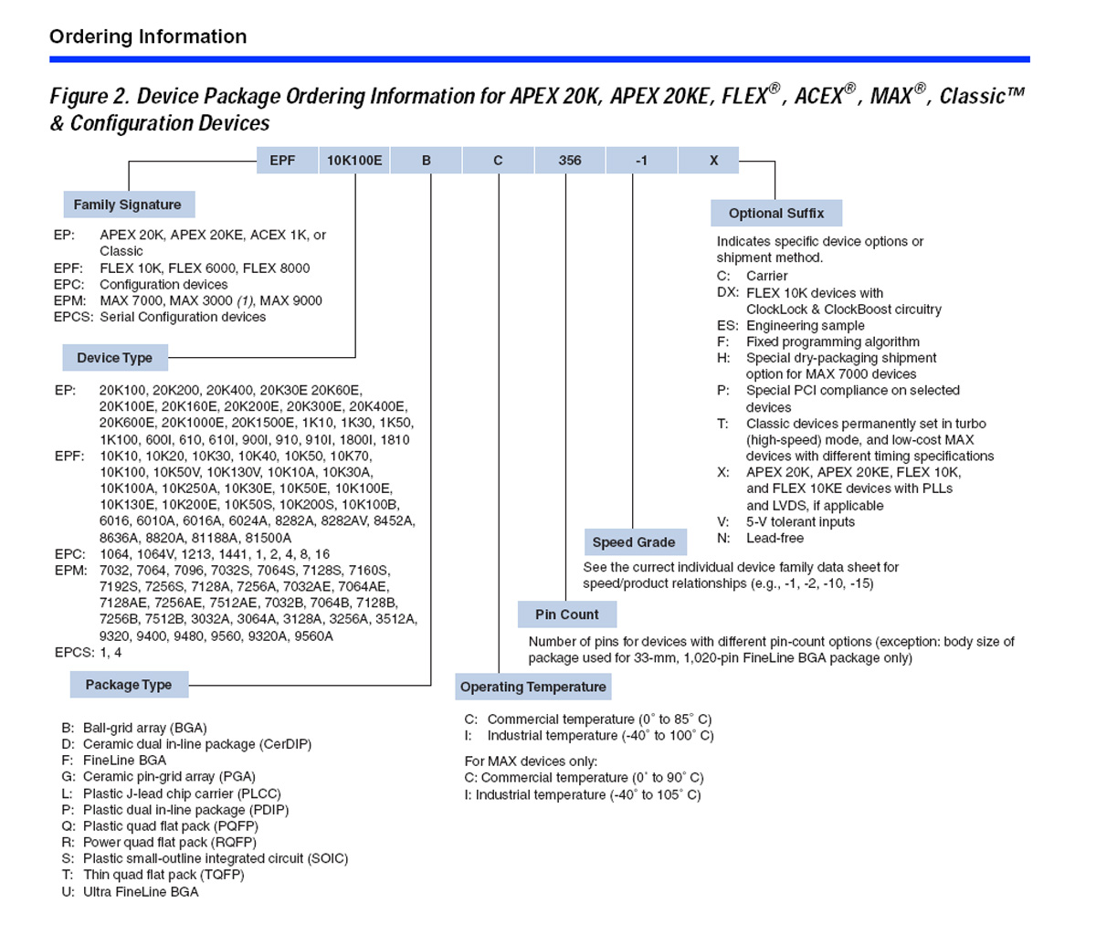
Altera MAX Part numbers Explained
If you've been confused by the Altera MAX part numbering system like "Altera Part# EPM7160SLC84-10"
Don't worry, most of us are confused at first. To make things easier for you I have provided the Altera part numbers description page (ordering codes) that is used for ordering parts from Altera. This is just really handy to have regardless where you are buying your chips from.
See the image below:
(From Altera Datasheet Dated 2001)
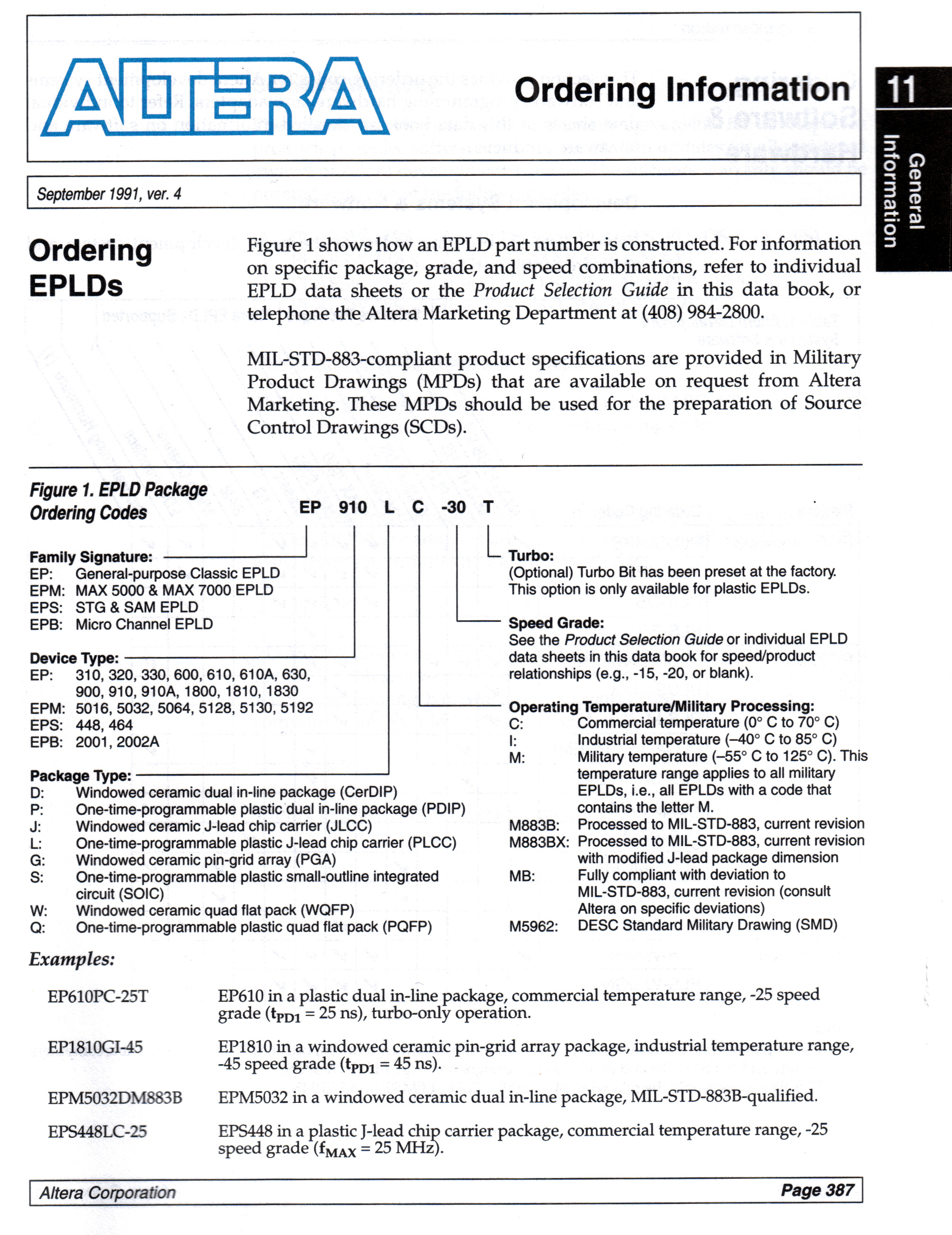
The Image below is the ordering info for the Older Classic Altera CPLD components like the Altera EP1810LC components
(From Databook Dated 1991)
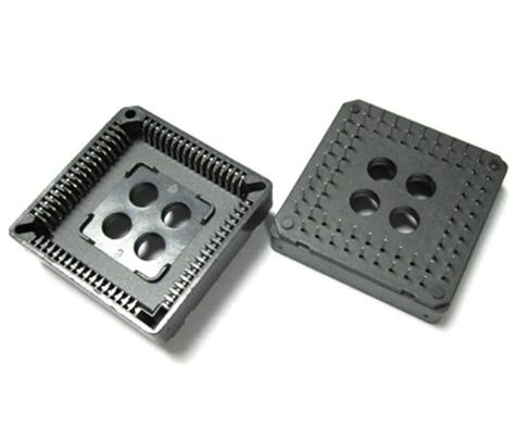
The Altera MAX "7000S" series CPLDs are one of the Altera components that support the JTAG interface and are therefore perfect for Hobbyists. Especially the components in the PLCC package format as I stated earlier. Modern components are so unbelievably small and are all surface mount devices which are not very practical for the average Joe to attempt any kind of soldering.
Soldering connections to a PLCC package device or socket is much more practical for the average Hobbyist.
Compared to some of the newer Surface mount or BGA package components.
Specialized equipment is needed for soldering these Devices and they are just too small to work with, unless you decide to invest in the specialized tools required.
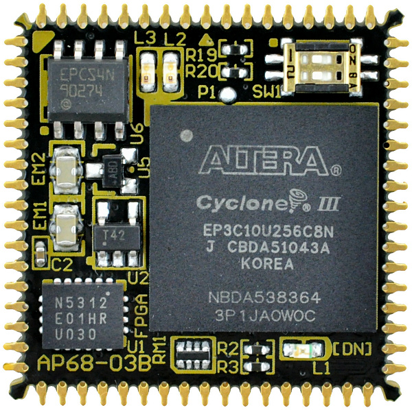
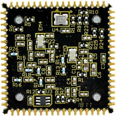
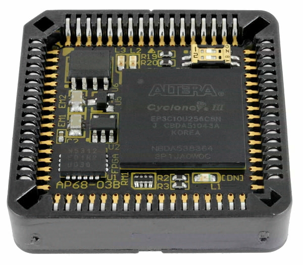
However, just recently the Company HuMANDATA Ltd. in Japan has released an Altera Cyclone III BGA chip in a PLCC-68 format.
See the images below.
This provides the sophisticated features of the Newer FPGA's yet still able to be plugged into standard PLCC-68 Sockets. FANATASTIC !!! See the Details and ordering info from the link Below:
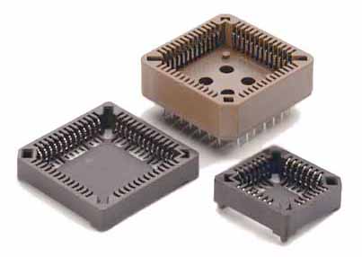
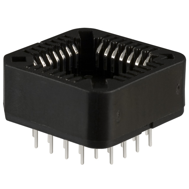
Using PLCC sockets allows you the freedom to quickly remove the CPLD from the circuit, in case you wish to try a different chip or program it in another system.
PLCC / CPLD "Through-Hole" Socket Pinouts
Another important and handy diagram to have is the CPLD / PLCC Socket Pinout Diagram for your target Device. There are many different packages of CPLD's and FPGA's to choose from and it all depends on how many I/O pins you plan to use in your Interfacing design.
Below are the Pinout Diagrams for standard "through hole" CPLD Sockets.
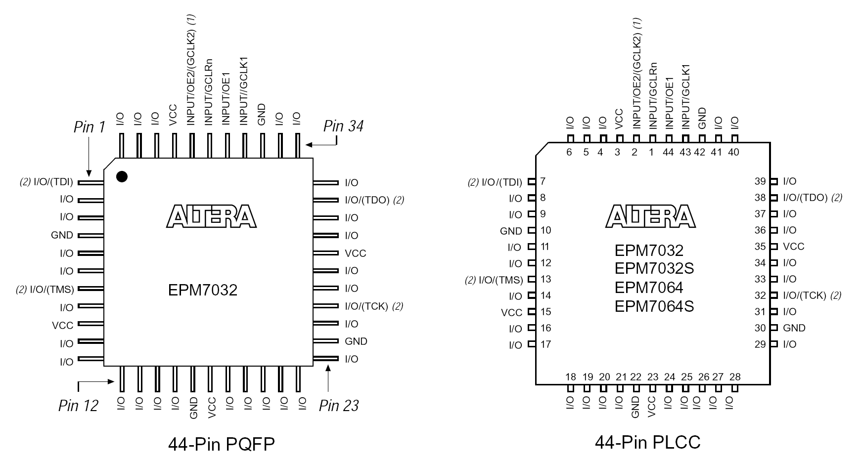
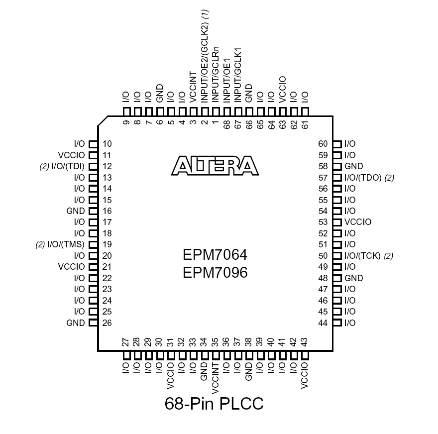
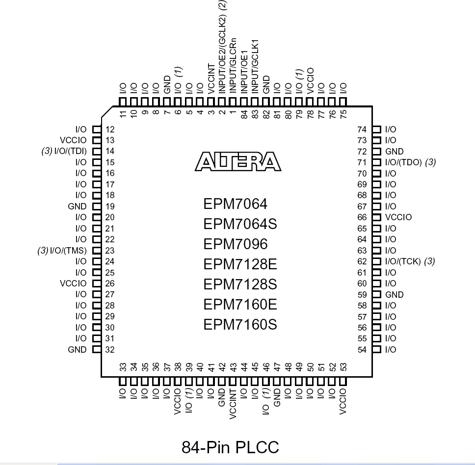
I also include the Pinouts for the Altera MAX series CPLD's for JTAG interfacing connections. Refer to the component datasheets to verify that your target device supports the JTAG interface. (Some Altera devices do not support JTAG)
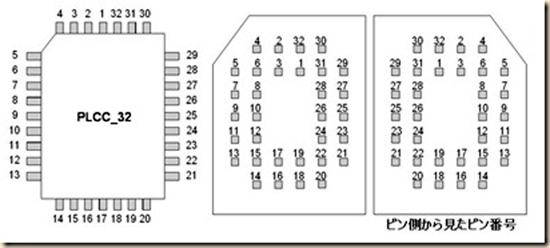
PLCC 32 Pin Socket Pinouts
For 4M-Bit Flash Chips
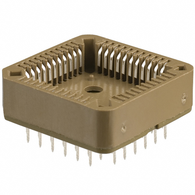
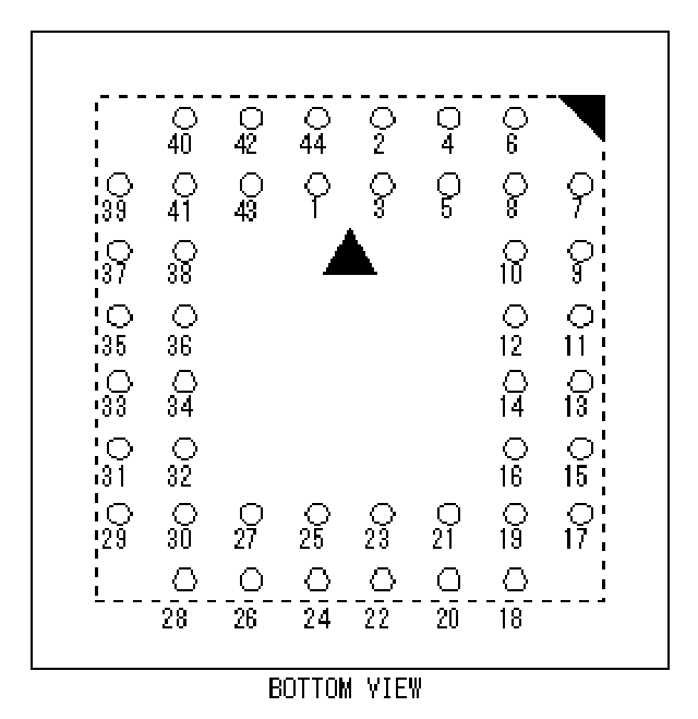
CPLD / PLCC 44 Pin Socket Pinouts
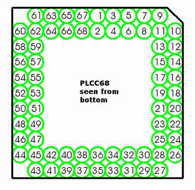
CPLD / PLCC 68 Pin Socket Pinouts
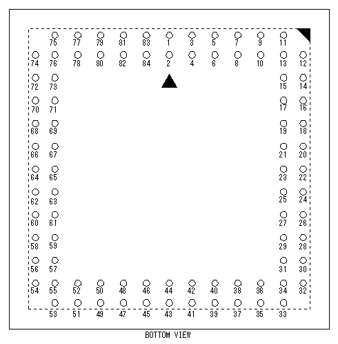
CPLD / PLCC 84 Pin Socket Pinouts
Also check out the Link below for the Altera USB-Blaster User's Manual:
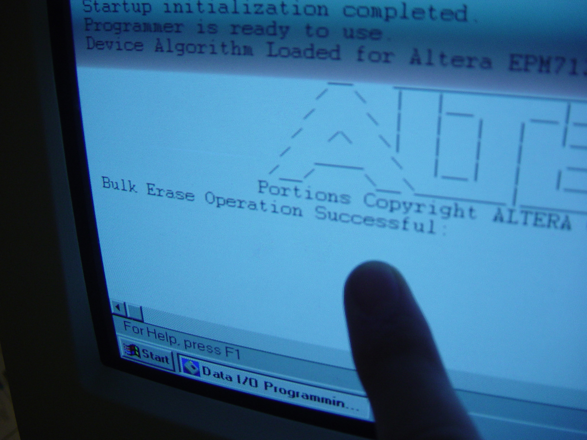
It is a common problem when students purchase Altera MAX CPLD's second hand off the internet, and they can't seem to program the chips via the JTAG Test-Access-Port.
Chances are the JTAG pins have been disabled and programmed to be used as Inputs or outputs. This doesn't happen all the time, and you might not have any problems at all. However, if you find a batch of chips you purchased on eBay, all seem to fail when trying to program them using a JTAG programmer; chances are the "JTAG INTERFACE" is disabled and it has to be reactivated by having the Chip reset or Erased by a Non-JTAG Master Programming unit or Universal Programmer.
This condition is known as "JTAG-LOCKOUT"
Many students run into this problem and believe the chip to be a dud or faulty. They will then buy a new chip and of course it works without issue. Sad thing is that there was probably nothing wrong with the other chip at all. The JTAG port was simply disabled. This condition is called "JTAG-LOCKOUT" and can only be reset by a Master programmer Unit or a Third party Universal Programmer like the DATA I/O Labsite, Unisite, 2900, 3980 and many other models and Brands that support Altera MAX CPLD components. Once the chip has been erased, it can then again be programmed through the "JTAG INTERFACE".
Please watch this detailed Video DEMO below of my
Altera Master Programming Units and other Altera JTAG Programming controllers.
If you're into the older Altera CPLD's you can Join my Altera Yahoo Group:


