|
Current Time:
|
|
|
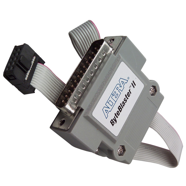
Gerry's Messy Electronics/Robotics Click the button below to go Back to the "CHIPPERY " section of my Lab ALTERA COMPONENT PINOUTS Below are the Pinout Diagrams for Altera USB-Blaster Programmer and various Altera CPLD and FPGA Logic Devices.
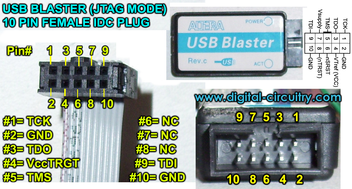
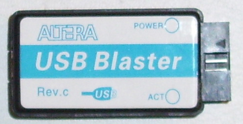
ALTERA JTAG USB-BLASTER ISP PROGRAMMER The Pinouts for the ALTERA USB-Blaster controller in the "JTAG IEEE 1532 Standard" Mode is shown in the image below.
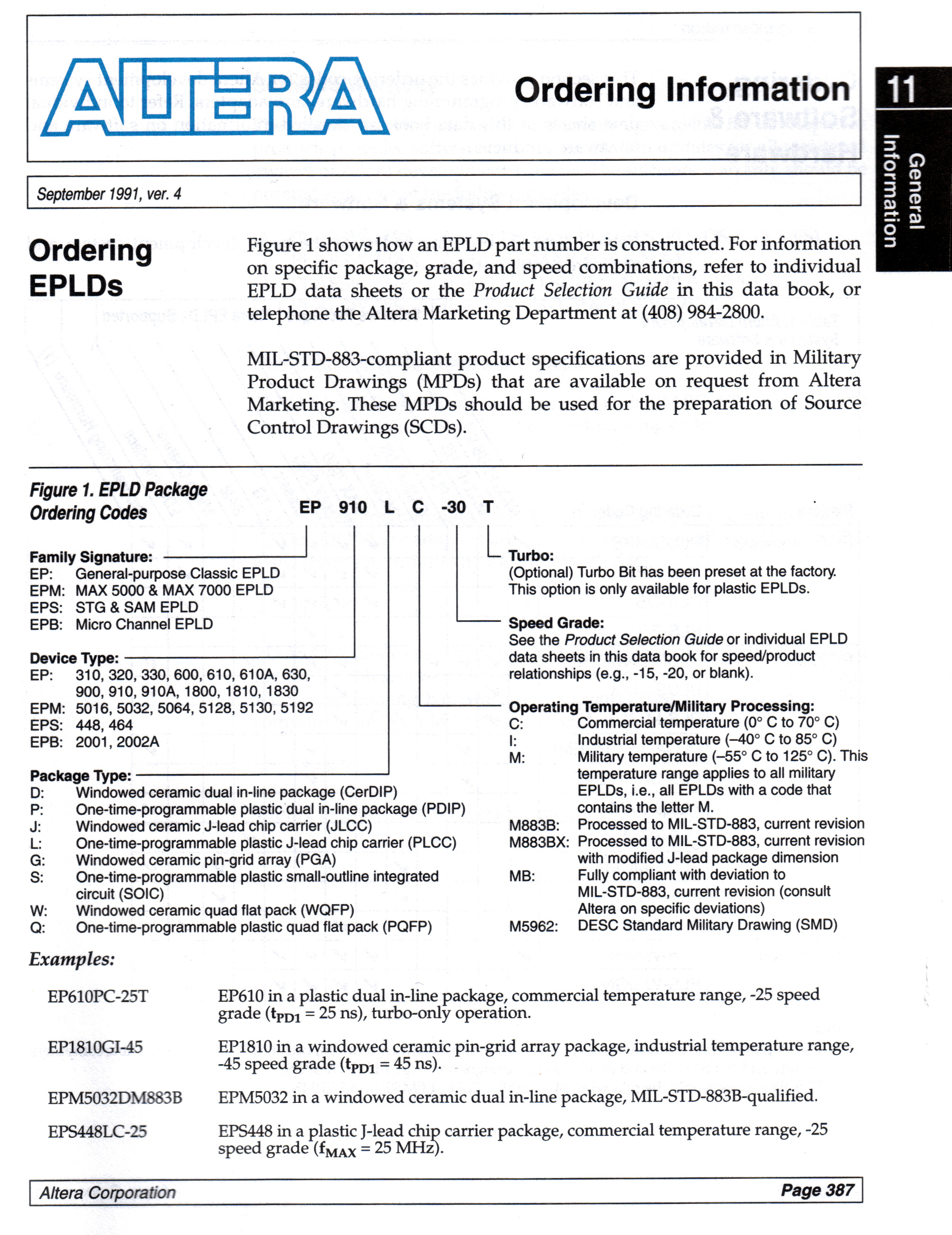
ALTERA COMPONENTS MODEL NUMBERS EXPLAINED Shown below are the Altera CPLD component ordering codes broken down to explain each section of the numbering system. This clearly indicates and explains the numbering system used for Altera CPLD components. The first Page is for the Altera CLASSIC Components dated 1991, The second page is for Altera MAX series dated 2001.
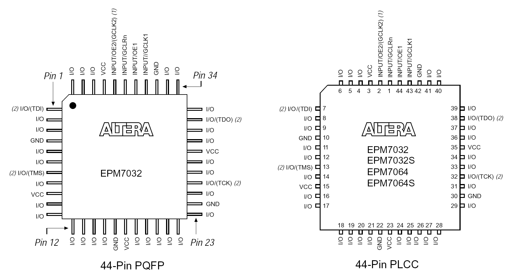
The Pinouts for the ALTERA MAX 7032 44-Pin PQFP & PLCC
The Pinouts for the ALTERA MAX 3032 44-Pin PQFP & PLCC
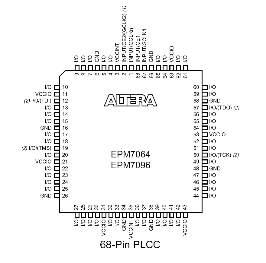
The Pinouts for the ALTERA MAX 7064 68-Pin PLCC
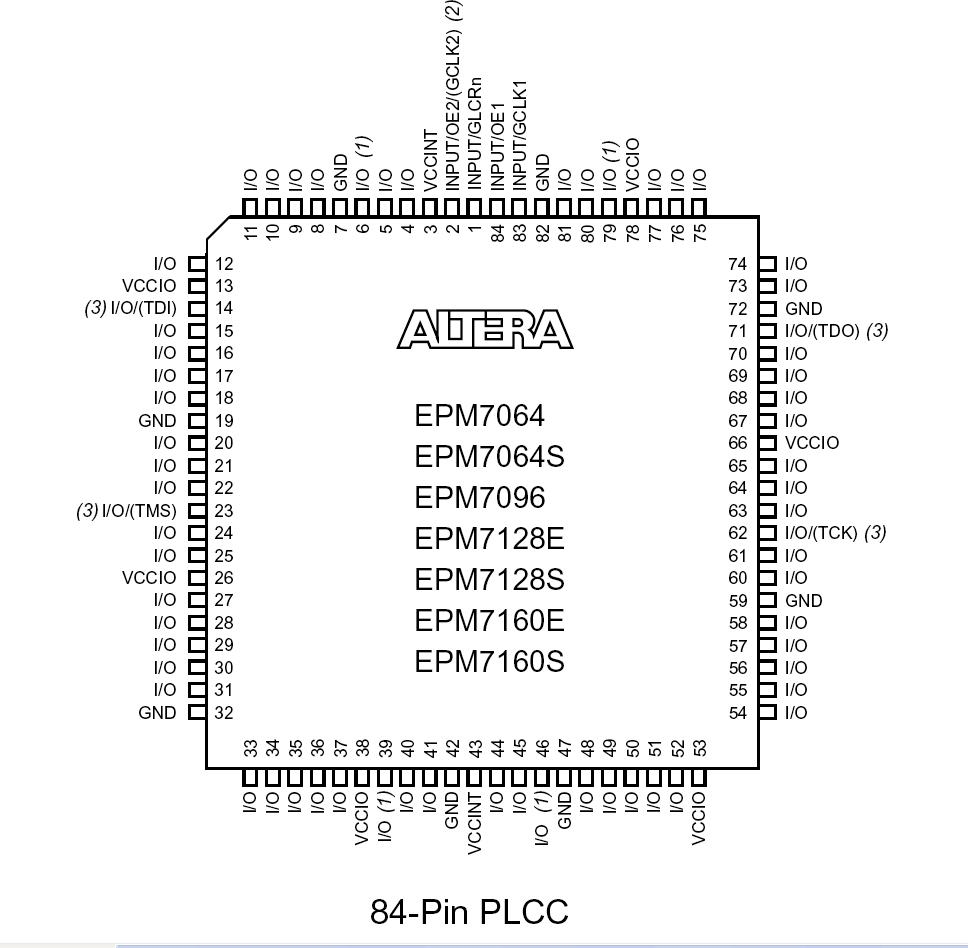
The Pinouts for the ALTERA MAX 7000 84-Pin PLCC
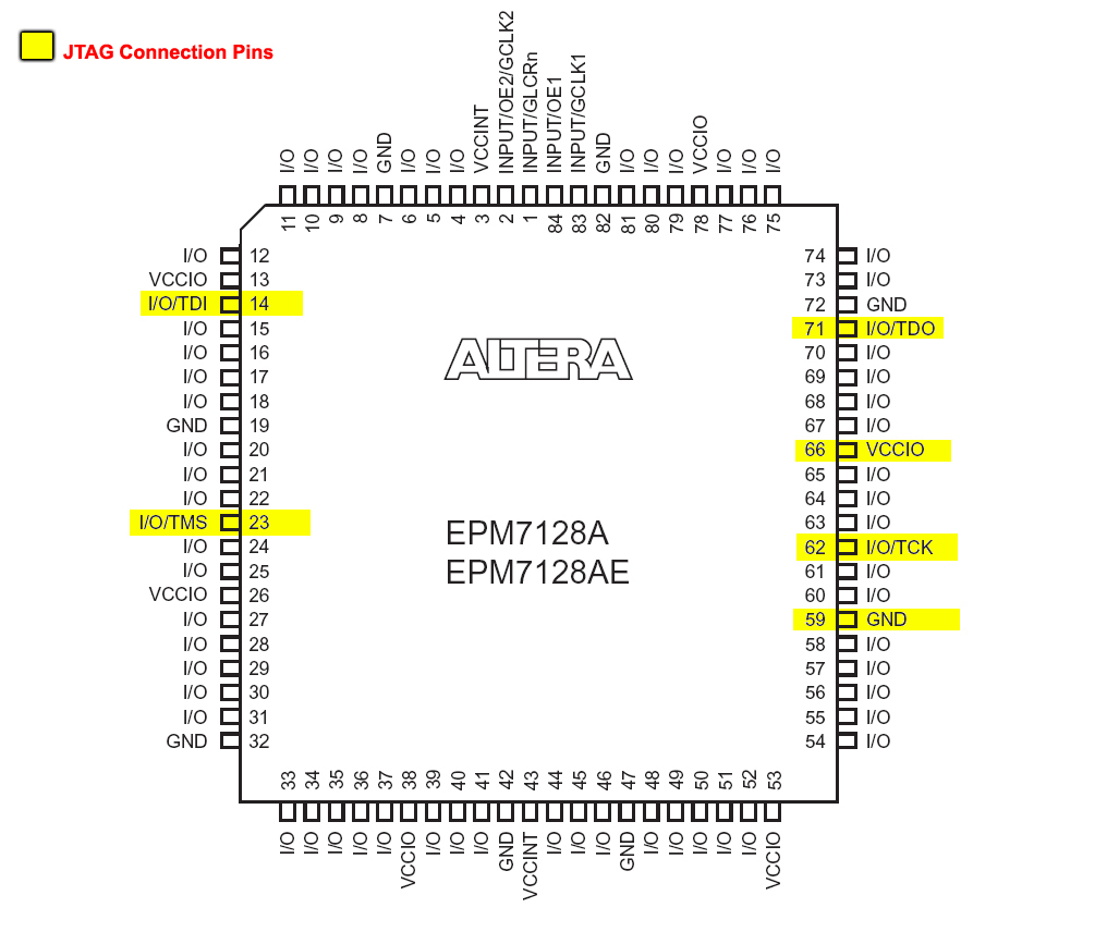
Altera MAX7000 "EPM7128SLC84" 84-Pin PLCC JTAG Pinout Diagram.
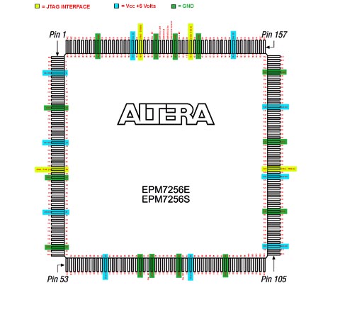
Altera MAX7000 "EPM7256SRC208" 208-Pin QFP Pinout Diagram. (HI-RES 2400 x 2200 Pixels PDF Document - 6.5 MB)
Also vist the Altera Website at the Link Below for Altera Device Pinout documents: http://www.altera.com/literature/lit-dp.jsp
For PLCC / CPLD "Through-Hole" Socket Pinouts and JTAG Interface info Visit the "JTAG ISP" Page
If you're into the older Altera CPLD's you can Join my Altera Yahoo Group: http://groups.yahoo.com/group/AlteraMAX7000/
Back to The "CHIPPERY" Section
|
||
|
||